ARM DMIPS算力说明
ARM算力参考官网地址
https://en.wikipedia.org/wiki/List_of_ARM_processors
| Product family | ARM architecture | Processor | Feature | Cache (I / D), MMU | Typical MIPS @ MHz | Reference |
|---|---|---|---|---|---|---|
| ARM1 | ARMv1 | ARM1 | First implementation | None | ||
| ARM2 | ARMv2 | ARM2 | ARMv2 added the MUL (multiply) instruction | None | 0.33 DMIPS/MHz | |
| ARM2aS | ARMv2a | ARM250 | Integrated MEMC (MMU), graphics and I/O processor. ARMv2a added the SWP and SWPB (swap) instructions | None, MEMC1a | ||
| ARM3 | First integrated memory cache | 4 KB unified | 0.50 DMIPS/MHz | |||
| ARM6 | ARMv3 | ARM60 | ARMv3 first to support 32-bit memory address space (previously 26-bit). ARMv3M first added long multiply instructions (32x32=64). | None | 10 MIPS @ 12 MHz | |
| ARM600 | As ARM60, cache and coprocessor bus (for FPA10 floating-point unit) | 4 KB unified | 28 MIPS @ 33 MHz | |||
| ARM610 | As ARM60, cache, no coprocessor bus | 4 KB unified | 17 MIPS @ 20 MHz 0.65 DMIPS/MHz | [4] | ||
| ARM7 | ARMv3 | ARM700 | coprocessor bus (for FPA11 floating-point unit) | 8 KB unified | 40 MHz | |
| ARM710 | As ARM700, no coprocessor bus | 8 KB unified | 40 MHz | [5] | ||
| ARM710a | As ARM710, also used as core of ARM7100 | 8 KB unified | 40 MHz 0.68 DMIPS/MHz | |||
| ARM7T | ARMv4T | ARM7TDMI(-S) | 3-stage pipeline, Thumb, ARMv4 first to drop legacy ARM 26-bit addressing | None | 15 MIPS @ 16.8 MHz 63 DMIPS @ 70 MHz | |
| ARM710T | As ARM7TDMI, cache | 8 KB unified, MMU | 36 MIPS @ 40 MHz | |||
| ARM720T | As ARM7TDMI, cache | 8 KB unified, MMU with FCSE (Fast Context Switch Extension) | 60 MIPS @ 59.8 MHz | |||
| ARM740T | As ARM7TDMI, cache | MPU | ||||
| ARM7EJ | ARMv5TEJ | ARM7EJ-S | 5-stage pipeline, Thumb, Jazelle DBX, enhanced DSP instructions | None | ||
| ARM8 | ARMv4 | ARM810 | 5-stage pipeline, static branch prediction, double-bandwidth memory | 8 KB unified, MMU | 84 MIPS @ 72 MHz 1.16 DMIPS/MHz | [6][7] |
| ARM9T | ARMv4T | ARM9TDMI | 5-stage pipeline, Thumb | None | ||
| ARM920T | As ARM9TDMI, cache | 16 KB / 16 KB, MMU with FCSE (Fast Context Switch Extension) | 200 MIPS @ 180 MHz | [8] | ||
| ARM922T | As ARM9TDMI, caches | 8 KB / 8 KB, MMU | ||||
| ARM940T | As ARM9TDMI, caches | 4 KB / 4 KB, MPU | ||||
| ARM9E | ARMv5TE | ARM946E-S | Thumb, enhanced DSP instructions, caches | Variable, tightly coupled memories, MPU | ||
| ARM966E-S | Thumb, enhanced DSP instructions | No cache, TCMs | ||||
| ARM968E-S | As ARM966E-S | No cache, TCMs | ||||
| ARMv5TEJ | ARM926EJ-S | Thumb, Jazelle DBX, enhanced DSP instructions | Variable, TCMs, MMU | 220 MIPS @ 200 MHz | ||
| ARMv5TE | ARM996HS | Clockless processor, as ARM966E-S | No caches, TCMs, MPU | |||
| ARM10E | ARMv5TE | ARM1020E | 6-stage pipeline, Thumb, enhanced DSP instructions, (VFP) | 32 KB / 32 KB, MMU | ||
| ARM1022E | As ARM1020E | 16 KB / 16 KB, MMU | ||||
| ARMv5TEJ | ARM1026EJ-S | Thumb, Jazelle DBX, enhanced DSP instructions, (VFP) | Variable, MMU or MPU | |||
| ARM11 | ARMv6 | ARM1136J(F)-S | 8-stage pipeline, SIMD, Thumb, Jazelle DBX, (VFP), enhanced DSP instructions, unaligned memory access | Variable, MMU | 740 @ 532–665 MHz (i.MX31 SoC), 400–528 MHz | [9] |
| ARMv6T2 | ARM1156T2(F)-S | 9-stage pipeline, SIMD, Thumb-2, (VFP), enhanced DSP instructions | Variable, MPU | [10] | ||
| ARMv6Z | ARM1176JZ(F)-S | As ARM1136EJ(F)-S | Variable, MMU + TrustZone | 965 DMIPS @ 772 MHz, up to 2,600 DMIPS with four processors | [11] | |
| ARMv6K | ARM11MPCore | As ARM1136EJ(F)-S, 1–4 core SMP | Variable, MMU | |||
| SecurCore | ARMv6-M | SC000 | As Cortex-M0 | 0.9 DMIPS/MHz | ||
| ARMv4T | SC100 | As ARM7TDMI | ||||
| ARMv7-M | SC300 | As Cortex-M3 | 1.25 DMIPS/MHz | |||
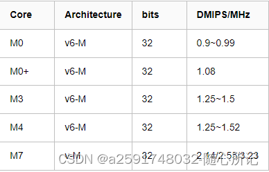
| Cortex-M | ARMv6-M | Cortex-M0 | Microcontroller profile, most Thumb + some Thumb-2,[12] hardware multiply instruction (optional small), optional system timer, optional bit-banding memory | Optional cache, no TCM, no MPU | 0.84 DMIPS/MHz | [13] |
| Cortex-M0+ | Microcontroller profile, most Thumb + some Thumb-2,[12] hardware multiply instruction (optional small), optional system timer, optional bit-banding memory | Optional cache, no TCM, optional MPU with 8 regions | 0.93 DMIPS/MHz | [14] | ||
| Cortex-M1 | Microcontroller profile, most Thumb + some Thumb-2,[12] hardware multiply instruction (optional small), OS option adds SVC / banked stack pointer, optional system timer, no bit-banding memory | Optional cache, 0–1024 KB I-TCM, 0–1024 KB D-TCM, no MPU | 136 DMIPS @ 170 MHz,[15] (0.8 DMIPS/MHz FPGA-dependent)[16] | [17] | ||
| ARMv7-M | Cortex-M3 | Microcontroller profile, Thumb / Thumb-2, hardware multiply and divide instructions, optional bit-banding memory | Optional cache, no TCM, optional MPU with 8 regions | 1.25 DMIPS/MHz | [18] | |
| ARMv7E-M | Cortex-M4 | Microcontroller profile, Thumb / Thumb-2 / DSP / optional VFPv4-SP single-precision FPU, hardware multiply and divide instructions, optional bit-banding memory | Optional cache, no TCM, optional MPU with 8 regions | 1.25 DMIPS/MHz (1.27 w/FPU) | [19] | |
| Cortex-M7 | Microcontroller profile, Thumb / Thumb-2 / DSP / optional VFPv5 single and double precision FPU, hardware multiply and divide instructions | 0−64 KB I-cache, 0−64 KB D-cache, 0–16 MB I-TCM, 0–16 MB D-TCM (all these w/optional ECC), optional MPU with 8 or 16 regions | 2.14 DMIPS/MHz | [20] | ||
| ARMv8-M Baseline | Cortex-M23 | Microcontroller profile, Thumb-1 (most), Thumb-2 (some), Divide, TrustZone | Optional cache, no TCM, optional MPU with 16 regions | 1.03 DMIPS/MHz | [21] | |
| ARMv8-M Mainline | Cortex-M33 | Microcontroller profile, Thumb-1, Thumb-2, Saturated, DSP, Divide, FPU (SP), TrustZone, Co-processor | Optional cache, no TCM, optional MPU with 16 regions | 1.50 DMIPS/MHz | [22] | |
| Cortex-M35P | Microcontroller profile, Thumb-1, Thumb-2, Saturated, DSP, Divide, FPU (SP), TrustZone, Co-processor | Built-in cache (with option 2–16 KB), I-cache, no TCM, optional MPU with 16 regions | 1.50 DMIPS/MHz | [23] | ||
| ARMv8.1-M Mainline | Cortex-M52 | 1.60 DMIPS/MHz | [24] | |||
| Cortex-M55 | 1.69 DMIPS/MHz | [25] | ||||
| Cortex-M85 | 3.13 DMIPS/MHz | [26] | ||||
| Cortex-R | ARMv7-R | Cortex-R4 | Real-time profile, Thumb / Thumb-2 / DSP / optional VFPv3 FPU, hardware multiply and optional divide instructions, optional parity & ECC for internal buses / cache / TCM, 8-stage pipeline dual-core running lockstep with fault logic | 0–64 KB / 0–64 KB, 0–2 of 0–8 MB TCM, opt. MPU with 8/12 regions | 1.67 DMIPS/MHz[27] | [28] |
| Cortex-R5 | Real-time profile, Thumb / Thumb-2 / DSP / optional VFPv3 FPU and precision, hardware multiply and optional divide instructions, optional parity & ECC for internal buses / cache / TCM, 8-stage pipeline dual-core running lock-step with fault logic / optional as 2 independent cores, low-latency peripheral port (LLPP), accelerator coherency port (ACP)[29] | 0–64 KB / 0–64 KB, 0–2 of 0–8 MB TCM, opt. MPU with 12/16 regions | 1.67 DMIPS/MHz[27] | [30] | ||
| Cortex-R7 | Real-time profile, Thumb / Thumb-2 / DSP / optional VFPv3 FPU and precision, hardware multiply and optional divide instructions, optional parity & ECC for internal buses / cache / TCM, 11-stage pipeline dual-core running lock-step with fault logic / out-of-order execution / dynamic register renaming / optional as 2 independent cores, low-latency peripheral port (LLPP), ACP[29] | 0–64 KB / 0–64 KB, ? of 0–128 KB TCM, opt. MPU with 16 regions | 2.50 DMIPS/MHz[27] | [31] | ||
| Cortex-R8 | TBD | 0–64 KB / 0–64 KB L1, 0–1 / 0–1 MB TCM, opt MPU with 24 regions | 2.50 DMIPS/MHz[27] | [32] | ||
| ARMv8-R | Cortex-R52 | TBD | 0–32 KB / 0–32 KB L1, 0–1 / 0–1 MB TCM, opt MPU with 24+24 regions | 2.09 DMIPS/MHz | [33] | |
| Cortex-R52+ | TBD | 0–32 KB / 0–32 KB L1, 0–1 / 0–1 MB TCM, opt MPU with 24+24 regions | 2.09 DMIPS/MHz | [34] | ||
| Cortex-R82 | TBD | 16–128 KB /16–64 KB L1, 64K–1MB L2, 0.16–1 / 0.16–1 MB TCM, opt MPU with 32+32 regions | 3.41 DMIPS/MHz[35] | [36] | ||
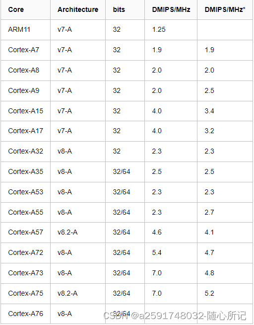
| Cortex-A(32-bit) | ARMv7-A | Cortex-A5 | Application profile, ARM / Thumb / Thumb-2 / DSP / SIMD / Optional VFPv4-D16 FPU / Optional NEON / Jazelle RCT and DBX, 1–4 cores / optional MPCore, snoop control unit (SCU), generic interrupt controller (GIC), accelerator coherence port (ACP) | 4−64 KB / 4−64 KB L1, MMU + TrustZone | 1.57 DMIPS/MHz per core | [37] |
| Cortex-A7 | Application profile, ARM / Thumb / Thumb-2 / DSP / VFPv4 FPU / NEON / Jazelle RCT and DBX / Hardware virtualization, in-order execution, superscalar, 1–4 SMP cores, MPCore, Large Physical Address Extensions (LPAE), snoop control unit (SCU), generic interrupt controller (GIC), architecture and feature set are identical to A15, 8–10 stage pipeline, low-power design[38] | 8−64 KB / 8−64 KB L1, 0–1 MB L2, MMU + TrustZone | 1.9 DMIPS/MHz per core | [39] | ||
| Cortex-A8 | Application profile, ARM / Thumb / Thumb-2 / VFPv3 FPU / NEON / Jazelle RCT and DAC, 13-stage superscalar pipeline | 16–32 KB / 16–32 KB L1, 0–1 MB L2 opt. ECC, MMU + TrustZone | Up to 2000 (2.0 DMIPS/MHz in speed from 600 MHz to greater than 1 GHz) | [40] | ||
| Cortex-A9 | Application profile, ARM / Thumb / Thumb-2 / DSP / Optional VFPv3 FPU / Optional NEON / Jazelle RCT and DBX, out-of-order speculative issue superscalar, 1–4 SMP cores, MPCore, snoop control unit (SCU), generic interrupt controller (GIC), accelerator coherence port (ACP) | 16–64 KB / 16–64 KB L1, 0–8 MB L2 opt. parity, MMU + TrustZone | 2.5 DMIPS/MHz per core, 10,000 DMIPS @ 2 GHz on Performance Optimized TSMC 40G (dual-core) | [41] | ||
| Cortex-A12 | Application profile, ARM / Thumb-2 / DSP / VFPv4 FPU / NEON / Hardware virtualization, out-of-order speculative issue superscalar, 1–4 SMP cores, Large Physical Address Extensions (LPAE), snoop control unit (SCU), generic interrupt controller (GIC), accelerator coherence port (ACP) | 32−64 KB | 3.0 DMIPS/MHz per core | [42] | ||
| Cortex-A15 | Application profile, ARM / Thumb / Thumb-2 / DSP / VFPv4 FPU / NEON / integer divide / fused MAC / Jazelle RCT / hardware virtualization, out-of-order speculative issue superscalar, 1–4 SMP cores, MPCore, Large Physical Address Extensions (LPAE), snoop control unit (SCU), generic interrupt controller (GIC), ACP, 15-24 stage pipeline[38] | 32 KB w/parity / 32 KB w/ECC L1, 0–4 MB L2, L2 has ECC, MMU + TrustZone | At least 3.5 DMIPS/MHz per core (up to 4.01 DMIPS/MHz depending on implementation)[43] | [44] | ||
| Cortex-A17 | Application profile, ARM / Thumb / Thumb-2 / DSP / VFPv4 FPU / NEON / integer divide / fused MAC / Jazelle RCT / hardware virtualization, out-of-order speculative issue superscalar, 1–4 SMP cores, MPCore, Large Physical Address Extensions (LPAE), snoop control unit (SCU), generic interrupt controller (GIC), ACP | 32 KB L1, 256 KB–8 MB L2 w/optional ECC | 2.8 DMIPS/MHz | [45] | ||
| ARMv8-A | Cortex-A32 | Application profile, AArch32, 1–4 SMP cores, TrustZone, NEON advanced SIMD, VFPv4, hardware virtualization, dual issue, in-order pipeline | 8–64 KB w/optional parity / 8−64 KB w/optional ECC L1 per core, 128 KB–1 MB L2 w/optional ECC shared | [46] | ||
| Cortex-A(64-bit) | ARMv8-A | Cortex-A34 | Application profile, AArch64, 1–4 SMP cores, TrustZone, NEON advanced SIMD, VFPv4, hardware virtualization, 2-width decode, in-order pipeline | 8−64 KB w/parity / 8−64 KB w/ECC L1 per core, 128 KB–1 MB L2 shared, 40-bit physical addresses | [47] | |
| Cortex-A35 | Application profile, AArch32 and AArch64, 1–4 SMP cores, TrustZone, NEON advanced SIMD, VFPv4, hardware virtualization, 2-width decode, in-order pipeline | 8−64 KB w/parity / 8−64 KB w/ECC L1 per core, 128 KB–1 MB L2 shared, 40-bit physical addresses | 1.78 DMIPS/MHz | [48] | ||
| Cortex-A53 | Application profile, AArch32 and AArch64, 1–4 SMP cores, TrustZone, NEON advanced SIMD, VFPv4, hardware virtualization, 2-width decode, in-order pipeline | 8−64 KB w/parity / 8−64 KB w/ECC L1 per core, 128 KB–2 MB L2 shared, 40-bit physical addresses | 2.3 DMIPS/MHz | [49] | ||
| Cortex-A57 | Application profile, AArch32 and AArch64, 1–4 SMP cores, TrustZone, NEON advanced SIMD, VFPv4, hardware virtualization, 3-width decode superscalar, deeply out-of-order pipeline | 48 KB w/DED parity / 32 KB w/ECC L1 per core; 512 KB–2 MB L2 shared w/ECC; 44-bit physical addresses | 4.1–4.8 DMIPS/MHz[50][51] | [52] | ||
| Cortex-A72 | Application profile, AArch32 and AArch64, 1–4 SMP cores, TrustZone, NEON advanced SIMD, VFPv4, hardware virtualization, 3-width superscalar, deeply out-of-order pipeline | 48 KB w/DED parity / 32 KB w/ECC L1 per core; 512 KB–2 MB L2 shared w/ECC; 44-bit physical addresses | 6.3-7.3 DMIPS/MHz[53] | [54] | ||
| Cortex-A73 | Application profile, AArch32 and AArch64, 1–4 SMP cores, TrustZone, NEON advanced SIMD, VFPv4, hardware virtualization, 2-width superscalar, deeply out-of-order pipeline | 64 KB / 32−64 KB L1 per core, 256 KB–8 MB L2 shared w/ optional ECC, 44-bit physical addresses | 7.4-8.5 DMIPS/MHz[53] | [55] | ||
| ARMv8.2-A | Cortex-A55 | Application profile, AArch32 and AArch64, 1–8 SMP cores, TrustZone, NEON advanced SIMD, VFPv4, hardware virtualization, 2-width decode, in-order pipeline[56] | 16−64 KB / 16−64 KB L1, 256 KB L2 per core, 4 MB L3 shared | 3 DMIPS/MHz[53] | [57] | |
| Cortex-A65 | Application profile, AArch64, 1–8 SMP cores, TrustZone, NEON advanced SIMD, VFPv4, hardware virtualization, 2-wide decode superscalar, 3-width issue, out-of-order pipeline, SMT | [58] | ||||
| Cortex-A65AE | As ARM Cortex-A65, adds dual core lockstep for safety applications | 64 / 64 KB L1, 256 KB L2 per core, 4 MB L3 shared | [59] | |||
| Cortex-A75 | Application profile, AArch32 and AArch64, 1–8 SMP cores, TrustZone, NEON advanced SIMD, VFPv4, hardware virtualization, 3-width decode superscalar, deeply out-of-order pipeline[60] | 64 / 64 KB L1, 512 KB L2 per core, 4 MB L3 shared | 8.2-9.5 DMIPS/MHz[53] | [61] | ||
| Cortex-A76 | Application profile, AArch32 (non-privileged level or EL0 only) and AArch64, 1–4 SMP cores, TrustZone, NEON advanced SIMD, VFPv4, hardware virtualization, 4-width decode superscalar, 8-way issue, 13 stage pipeline, deeply out-of-order pipeline[62] | 64 / 64 KB L1, 256−512 KB L2 per core, 512 KB−4 MB L3 shared | 10.7-12.4 DMIPS/MHz[53] | [63] | ||
| Cortex-A76AE | As ARM Cortex-A76, adds dual core lockstep for safety applications | [64] | ||||
| Cortex-A77 | Application profile, AArch32 (non-privileged level or EL0 only) and AArch64, 1–4 SMP cores, TrustZone, NEON advanced SIMD, VFPv4, hardware virtualization, 4-width decode superscalar, 6-width instruction fetch, 12-way issue, 13 stage pipeline, deeply out-of-order pipeline[62] | 1.5K L0 MOPs cache, 64 / 64 KB L1, 256−512 KB L2 per core, 512 KB−4 MB L3 shared | 13-16 DMIPS/MHz[65] | [66] | ||
| Cortex-A78 | [67] | |||||
| Cortex-A78AE | As ARM Cortex-A78, adds dual core lockstep for safety applications | [68] | ||||
| Cortex-A78C | [69] | |||||
| ARMv9-A | Cortex-A510 | |||||
| Cortex-A710 | [70] | |||||
| Cortex-A715 | ||||||
| Cortex-A520 | ||||||
| Cortex-A720 | ||||||
| Cortex-X | ARMv8.2-A | Cortex-X1 | Performance-tuned variant of Cortex-A78 | |||
| ARMv9-A | Cortex-X2 | |||||
| Cortex-X3 | ||||||
| Cortex-X4 | ||||||
| Neoverse | ARMv8.2-A | Neoverse N1 | Application profile, AArch32 (non-privileged level or EL0 only) and AArch64, 1–4 SMP cores, TrustZone, NEON advanced SIMD, VFPv4, hardware virtualization, 4-width decode superscalar, 8-way dispatch/issue, 13 stage pipeline, deeply out-of-order pipeline[62] | 64 / 64 KB L1, 512−1024 KB L2 per core, 2−128 MB L3 shared, 128 MB system level cache | [71] | |
| Neoverse E1 | Application profile, AArch64, 1–8 SMP cores, TrustZone, NEON advanced SIMD, VFPv4, hardware virtualization, 2-wide decode superscalar, 3-width issue, 10 stage pipeline, out-of-order pipeline, SMT | 32−64 KB / 32−64 KB L1, 256 KB L2 per core, 4 MB L3 shared | [72] | |||
| ARMv8.4-A | Neoverse V1 | [73] | ||||
| ARMv9-A | Neoverse N2 | [74] | ||||
| ARM family | ARM architecture | ARM core | Feature | Cache (I / D), MMU | Typical MIPS @ MHz | Reference |
Designed by third parties[edit]
These cores implement the ARM instruction set, and were developed independently by companies with an architectural license from ARM.
| Product family | ARM architecture | Processor | Feature | Cache (I / D), MMU | Typical MIPS @ MHz |
|---|---|---|---|---|---|
| StrongARM (Digital) | ARMv4 | SA-110 | 5-stage pipeline | 16 KB / 16 KB, MMU | 100–233 MHz 1.0 DMIPS/MHz |
| SA-1100 | derivative of the SA-110 | 16 KB / 8 KB, MMU | |||
| Faraday[75] (Faraday Technology) | ARMv4 | FA510 | 6-stage pipeline | Up to 32 KB / 32 KB cache, MPU | 1.26 DMIPS/MHz 100–200 MHz |
| FA526 | Up to 32 KB / 32 KB cache, MMU | 1.26 MIPS/MHz 166–300 MHz | |||
| FA626 | 8-stage pipeline | 32 KB / 32 KB cache, MMU | 1.35 DMIPS/MHz 500 MHz | ||
| ARMv5TE | FA606TE | 5-stage pipeline | No cache, no MMU | 1.22 DMIPS/MHz 200 MHz | |
| FA626TE | 8-stage pipeline | 32 KB / 32 KB cache, MMU | 1.43 MIPS/MHz 800 MHz | ||
| FMP626TE | 8-stage pipeline, SMP | 1.43 MIPS/MHz 500 MHz | |||
| FA726TE | 13 stage pipeline, dual issue | 2.4 DMIPS/MHz 1000 MHz | |||
| XScale (Intel / Marvell) | ARMv5TE | XScale | 7-stage pipeline, Thumb, enhanced DSP instructions | 32 KB / 32 KB, MMU | 133–400 MHz |
| Bulverde | Wireless MMX, wireless SpeedStep added | 32 KB / 32 KB, MMU | 312–624 MHz | ||
| Monahans[76] | Wireless MMX2 added | 32 KB / 32 KB L1, optional L2 cache up to 512 KB, MMU | Up to 1.25 GHz | ||
| Sheeva (Marvell) | ARMv5 | Feroceon | 5–8 stage pipeline, single-issue | 16 KB / 16 KB, MMU | 600–2000 MHz |
| Jolteon | 5–8 stage pipeline, dual-issue | 32 KB / 32 KB, MMU | |||
| PJ1 (Mohawk) | 5–8 stage pipeline, single-issue, Wireless MMX2 | 32 KB / 32 KB, MMU | 1.46 DMIPS/MHz 1.06 GHz | ||
| ARMv6 / ARMv7-A | PJ4 | 6–9 stage pipeline, dual-issue, Wireless MMX2, SMP | 32 KB / 32 KB, MMU | 2.41 DMIPS/MHz 1.6 GHz | |
| Snapdragon (Qualcomm) | ARMv7-A | Scorpion[77] | 1 or 2 cores. ARM / Thumb / Thumb-2 / DSP / SIMD / VFPv3 FPU / NEON (128-bit wide) | 256 KB L2 per core | 2.1 DMIPS/MHz per core |
| Krait[77] | 1, 2, or 4 cores. ARM / Thumb / Thumb-2 / DSP / SIMD / VFPv4 FPU / NEON (128-bit wide) | 4 KB / 4 KB L0, 16 KB / 16 KB L1, 512 KB L2 per core | 3.3 DMIPS/MHz per core | ||
| ARMv8-A | Kryo[78] | 4 cores. | ? | Up to 2.2 GHz (6.3 DMIPS/MHz) | |
| Ax (Apple) | ARMv7-A | Swift[79] | 2 cores. ARM / Thumb / Thumb-2 / DSP / SIMD / VFPv4 FPU / NEON | L1: 32 KB / 32 KB, L2: 1 MB shared | 3.5 DMIPS/MHz per core |
| ARMv8-A | Cyclone[80] | 2 cores. ARM / Thumb / Thumb-2 / DSP / SIMD / VFPv4 FPU / NEON / TrustZone / AArch64. Out-of-order, superscalar. | L1: 64 KB / 64 KB, L2: 1 MB shared SLC: 4 MB | 1.3 or 1.4 GHz | |
| ARMv8-A | Typhoon[80][81] | 2 or 3 cores. ARM / Thumb / Thumb-2 / DSP / SIMD / VFPv4 FPU / NEON / TrustZone / AArch64 | L1: 64 KB / 64 KB, L2: 1 MB or 2 MB shared SLC: 4 MB | 1.4 or 1.5 GHz | |
| ARMv8-A | Twister[82] | 2 cores. ARM / Thumb / Thumb-2 / DSP / SIMD / VFPv4 FPU / NEON / TrustZone / AArch64 | L1: 64 KB / 64 KB, L2: 2 MB shared SLC: 4 MB or 0 MB | 1.85 or 2.26 GHz | |
| ARMv8-A | Hurricane and Zephyr[83] | Hurricane: 2 or 3 cores. AArch64, out-of-order, superscalar, 6-decode, 6-issue, 9-wide Zephyr: 2 or 3 cores. AArch64, out-of-order, superscalar. | L1: 64 KB / 64 KB, L2: 3 MB or 8 MB shared L1: 32 KB / 32 KB. L2: none SLC: 4 MB or 0 MB | 2.34 or 2.38 GHz 1.05 GHz | |
| ARMv8.2-A | Monsoon and Mistral[84] | Monsoon: 2 cores. AArch64, out-of-order, superscalar, 7-decode, ?-issue, 11-wide Mistral: 4 cores. AArch64, out-of-order, superscalar. Based on Swift. | L1I: 128 KB, L1D: 64 KB, L2: 8 MB shared L1: 32 KB / 32 KB, L2: 1 MB shared SLC: 4 MB | 2.39 GHz 1.70 GHz | |
| ARMv8.3-A | Vortex and Tempest[85] | Vortex: 2 or 4 cores. AArch64, out-of-order, superscalar, 7-decode, ?-issue, 11-wide Tempest: 4 cores. AArch64, out-of-order, superscalar, 3-decode. Based on Swift. | L1: 128 KB / 128 KB, L2: 8 MB shared L1: 32 KB / 32 KB, L2: 2 MB shared SLC: 8 MB | 2.49 GHz 1.59 GHz | |
| ARMv8.4-A | Lightning and Thunder[86] | Lightning: 2 cores. AArch64, out-of-order, superscalar, 7-decode, ?-issue, 11-wide Thunder: 4 cores. AArch64, out-of-order, superscalar. | L1: 128 KB / 128 KB, L2: 8 MB shared L1: 32 KB / 48 KB, L2: 4 MB shared SLC: 16 MB | 2.66 GHz 1.73 GHz | |
| ARMv8.5-A | Firestorm and Icestorm[87] | Firestorm: 2 cores. AArch64, out-of-order, superscalar, 8-decode, ?-issue, 14-wide Icestorm: 4 cores. AArch64, out-of-order, superscalar, 4-decode, ?-issue, 7-wide. | L1: 192 KB / 128 KB, L2: 8 MB shared L1: 128 KB / 64 KB, L2: 4 MB shared SLC: 16 MB | 3.0 GHz 1.82 GHz | |
| ARMv8.5-A | Avalanche and Blizzard | Avalanche: 2 cores. AArch64, out-of-order, superscalar, 8-decode, ?-issue, 14-wide Blizzard: 4 cores. AArch64, out-of-order, superscalar, 4-decode, ?-issue, 8-wide. | L1: 192 KB / 128 KB, L2: 12 MB shared L1: 128 KB / 64 KB, L2: 4 MB shared SLC: 32 MB | 2.93 or 3.23 GHz 2.02 GHz | |
| ARMv8.5-A | Everest and Sawtooth | Everest: 2 cores. AArch64, out-of-order, superscalar, 8-decode, ?-issue, 14-wide Sawtooth: 4 cores. AArch64, out-of-order, superscalar, 4-decode, ?-issue, 8-wide. | L1: 192 KB / 128 KB, L2: 16 MB shared L1: 128 KB / 64 KB, L2: 4 MB shared SLC: 24 MB | 3.46 GHz 2.02 GHz | |
| Mx (Apple) | ARMv8.4-A | Firestorm and Icestorm | Firestorm: 4, 6, 8 or 16 cores. AArch64, out-of-order, superscalar, 8-decode, ?-issue, 14-wide Icestorm: 2 or 4 cores. AArch64, out-of-order, superscalar, 4-decode, ?-issue, 7-wide. | L1: 192 KB / 128 KB, L2: 12, 24 or 48 MB shared L1: 128 KB / 64 KB, L2: 4 or 8 MB shared SLC: 8, 24, 48 or 96 MB | 3.2-3.23 GHz 2.06 GHz |
| ARMv8.5-A | Avalanche and Blizzard | Avalanche: 4, 6, 8 or 16 cores. AArch64, out-of-order, superscalar, 8-decode, ?-issue, 14-wide Blizzard: 4 or 8 cores. AArch64, out-of-order, superscalar, 4-decode, ?-issue, 8-wide. | L1: 192 KB / 128 KB, L2: 16, 32 or 64 MB shared L1: 128 KB / 64 KB, L2: 4 or 8 MB shared SLC: 8, 24, 48 or 96 MB | 3.49 GHz 2.42 GHz | |
| X-Gene (Applied Micro) | ARMv8-A | X-Gene | 64-bit, quad issue, SMP, 64 cores[88] | Cache, MMU, virtualization | 3 GHz (4.2 DMIPS/MHz per core) |
| Denver (Nvidia) | ARMv8-A | Denver[89][90] | 2 cores. AArch64, 7-wide superscalar, in-order, dynamic code optimization, 128 MB optimization cache, Denver1: 28 nm, Denver2:16 nm | 128 KB I-cache / 64 KB D-cache | Up to 2.5 GHz |
| Carmel (Nvidia) | ARMv8.2-A | Carmel[91][92] | 2 cores. AArch64, 10-wide superscalar, in-order, dynamic code optimization, ? MB optimization cache, functional safety, dual execution, parity & ECC | ? KB I-cache / ? KB D-cache | Up to ? GHz |
| ThunderX (Cavium) | ARMv8-A | ThunderX | 64-bit, with two models with 8–16 or 24–48 cores (×2 w/two chips) | ? | Up to 2.2 GHz |
| K12 (AMD) | ARMv8-A | K12[93] | ? | ? | ? |
| Exynos (Samsung) | ARMv8-A | M1 ("Mongoose")[94] | 4 cores. AArch64, 4-wide, quad-issue, superscalar, out-of-order | 64 KB I-cache / 32 KB D-cache, L2: 16-way shared 2 MB | 5.1 DMIPS/MHz (2.6 GHz) |
| ARMv8-A | M2 ("Mongoose") | 4 cores. AArch64, 4-wide, quad-issue, superscalar, out-of-order | 64 KB I-cache / 32 KB D-cache, L2: 16-way shared 2 MB | 2.3 GHz | |
| ARMv8-A | M3 ("Meerkat")[95] | 4 cores, AArch64, 6-decode, 6-issue, 6-wide. superscalar, out-of-order | 64 KB I-cache / 64 KB D-cache, L2: 8-way private 512 KB, L3: 16-way shared 4 MB | 2.7 GHz | |
| ARMv8.2-A | M4 ("Cheetah")[96] | 2 cores, AArch64, 6-decode, 6-issue, 6-wide. superscalar, out-of-order | 64 KB I-cache / 64 KB D-cache, L2: 8-way private 1 MB, L3: 16-way shared 3 MB | 2.73 GHz | |
| ARMv8.2-A | M5 ("Lion") | 2 cores, AArch64, 6-decode, 6-issue, 6-wide. superscalar, out-of-order | 64 KB I-cache / 64 KB D-cache, L2: 8-way shared 2 MB, L3: 12-way shared 3 MB | 2.73 GHz |
Timeline[edit]
The following table lists each core by the year it was announced.[97][98]
| Year | Classic cores | Cortex cores | Neoverse cores | ||||||||
|---|---|---|---|---|---|---|---|---|---|---|---|
| ARM1-6 | ARM7 | ARM8 | ARM9 | ARM10 | ARM11 | Microcontroller | Real-time | Application (32-bit) | Application (64-bit) | Application (64-bit) | |
| 1985 | ARM1 | ||||||||||
| 1986 | ARM2 | ||||||||||
| 1989 | ARM3 | ||||||||||
| 1992 | ARM250 | ||||||||||
| 1993 | ARM60 ARM610 | ARM700 | |||||||||
| 1994 | ARM710 ARM7DI ARM7TDMI | ||||||||||
| 1995 | ARM710a | ||||||||||
| 1996 | ARM810 | ||||||||||
| 1997 | ARM710T ARM720T ARM740T | ||||||||||
| 1998 | ARM9TDMI ARM940T | ||||||||||
| 1999 | ARM9E-S ARM966E-S | ||||||||||
| 2000 | ARM920T ARM922T ARM946E-S | ARM1020T | |||||||||
| 2001 | ARM7TDMI-S ARM7EJ-S | ARM9EJ-S ARM926EJ-S | ARM1020E ARM1022E | ||||||||
| 2002 | ARM1026EJ-S | ARM1136J(F)-S | |||||||||
| 2003 | ARM968E-S | ARM1156T2(F)-S ARM1176JZ(F)-S | |||||||||
| 2004 | Cortex-M3 | ||||||||||
| 2005 | ARM11MPCore | Cortex-A8 | |||||||||
| 2006 | ARM996HS | ||||||||||
| 2007 | Cortex-M1 | Cortex-A9 | |||||||||
| 2008 | |||||||||||
| 2009 | Cortex-M0 | Cortex-A5 | |||||||||
| 2010 | Cortex-M4(F) | Cortex-A15 | |||||||||
| 2011 | Cortex-R4 Cortex-R5 Cortex-R7 | Cortex-A7 | |||||||||
| 2012 | Cortex-M0+ | Cortex-A53 Cortex-A57 | |||||||||
| 2013 | Cortex-A12 | ||||||||||
| 2014 | Cortex-M7(F) | Cortex-A17 | |||||||||
| 2015 | Cortex-A35 Cortex-A72 | ||||||||||
| 2016 | Cortex-M23 Cortex-M33(F) | Cortex-R8 Cortex-R52 | Cortex-A32 | Cortex-A73 | |||||||
| 2017 | Cortex-A55 Cortex-A75 | ||||||||||
| 2018 | Cortex-M35P(F) | Cortex-A65AE Cortex-A76 Cortex-A76AE | |||||||||
| 2019 | Cortex-A77 | Neoverse E1 Neoverse N1 | |||||||||
| 2020 | Cortex-M55(F) | Cortex-R82 | Cortex-A78 Cortex-X1[99] | Neoverse V1[100] | |||||||
| 2021 | Cortex-A510 Cortex-A710 Cortex-X2 | Neoverse N2 | |||||||||
| 2022 | Cortex-M85(F) | Cortex-R52+ | Cortex-A715 Cortex-X3 | ||||||||
| 2023 | Cortex-M52(F) | Cortex-A520 Cortex-A720 Cortex-X4 | |||||||||
| 2024 | Cortex-R82AE | Cortex-A520AE Cortex-A720AE | Neoverse N3 Neoverse V3 Neoverse V3AE | ||||||||